
The Basic Structure and Principles of poe Network Transformers
2026-06-09
In wired LANs, computers, servers, hubs, routers, and other devices are connected using unshielded twisted pair (UTP) cables with a characteristic impedance close to 100Ω. Since servers, computers, and routers may be installed on different floors of a single building or across multiple buildings, the connecting cable lengths can extend to dozens or even hundreds of meters.
If computers, servers, or routers located tens of meters apart are directly connected with UTP, there are no issues when transmitting data signals between them. However, due to varying usage environments, various effects may arise.
If computers, servers, or routers located tens of meters apart are directly connected with UTP, there are no issues when transmitting data signals between them. However, due to varying usage environments, various effects may arise.
- Different reference levels
Due to differences in ground potential across various locations, a very low-frequency slowly varying voltage forms across the UTP cables and is directly applied to the integrated circuit chip of the network card, which may damage the chip.
- Poor electromagnetic interference resistance
A nearly 100-meter-long network cable is equivalent to a very long antenna. External electromagnetic interference (including lightning interference of several thousand volts) can enter the network card through the cable, potentially causing bit errors in the transmitted data signal. In severe cases, it may even damage the PHY chip.
- Strong external radiation
Electromagnetic interference (EMI) detected on UTP may cause bit errors in the transmitted data signals. Electromagnetic noise generated by switching power supplies and clock signal generators inside servers and computers will also be emitted into the surrounding space through UTP, forming interference sources for other electronic devices.
- Impedance mismatch
The characteristic impedance of cables and twisted pairs is fixed. To ensure signal integrity (SI), the internal resistance of the signal source, the load resistance, and the characteristic impedance of the twisted pair must match. Otherwise, both ends of the network cable must be matched. Impedance mismatch will cause reflections, potentially leading to bit errors in the transmitted data signal.
To address the aforementioned issues, a device is required between the UTP and PHY chips for signal coupling, high-voltage isolation, impedance matching, and electromagnetic interference suppression. This device is the network transformer.
The working principle of a network transformer
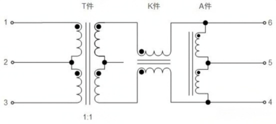
The network transformer consists of three components: the T piece (Transformer), the K piece (Common Mode Choke), and the A piece (Center Tapped Auto-Transformer).
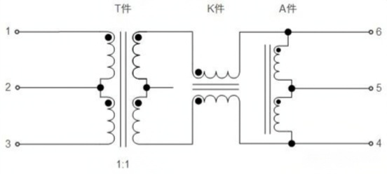
According to different combinations, network transformers can also be divided into: single T-piece network transformers, T-piece+K-piece network transformers, T-piece+three wire loop K-piece network transformers, and T-piece+K-piece+A-piece network transformers.
- Single T-piece network transformer
A single T-piece network transformer consists of two 1:1 coils with a center tap. The schematic diagram of the T-piece network transformer connected to UTP in actual use is shown in the figure. The hollow arrows in the figure indicate the direction of data signal transmission, while the solid arrows indicate the direction of data signal current.
According to the electromagnetic coupling principle of transformers, when a balanced signal is applied to twisted pair cables (UTP), an equivalent signal can be induced on the primary side of the transformer without loss, thereby achieving signal transmission.
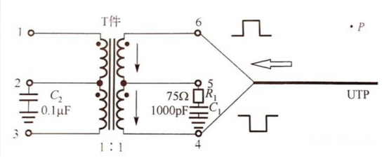
In addition, T-piece network transformers can block the mutual propagation of EMI between their primary and secondary coils. From Figure 3, it can be seen that the voltage waveforms of EMI on Pin 6 and Pin 4 have equal amplitudes and directions. Therefore, the currents in the upper and lower coils of the secondary are equal in magnitude and opposite in direction. The magnetic flux changes caused by the two currents inside the magnetic ring cancel each other out, and the magnetic flux change is zero, which means that the inductance presented by the upper and lower coils of the secondary is zero.
At this point, imagine the two coils above and below the secondary as a short circuit, and EMI interference will be discharged to the ground through the series circuit of the short circuit, the middle tap, R1, and C1 to dissipate the EMI induced on the UTP.
Similarly, EMI from the switching power supply, clock generator, and other circuits on the primary coil side will be discharged to the ground through the middle tap and C2 of the primary coil, which can reduce the EMI of the internal circuits of the primary coil and emit electromagnetic waves into the air through UTP.
It can be seen that the network transformer with a center tap has the function of blocking EMI from propagating between its primary and secondary coils.
- A network transformer composed of T and K components
As shown in the figure, it is a network transformer composed of T and K components.
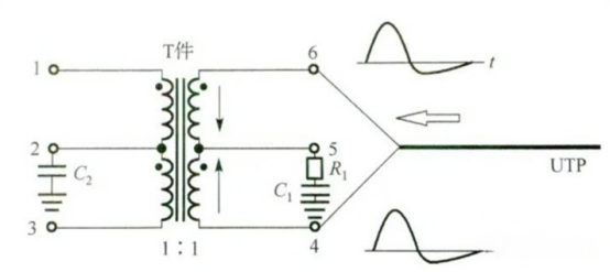
Due to the parasitic capacitance of non ideal transformers, some electromagnetic interference signals will be coupled to the primary end of the transformer through parasitic capacitance. Therefore, in order to further prevent electromagnetic interference from propagating between the primary and secondary coils, a single T-piece network transformer can be used, and then K pieces can be connected in series to the primary or secondary side of the transformer. This is a T-piece+K-piece network transformer.
Adding K components to the network transformer is because K components do not attenuate useful data voltage signals, but can attenuate EMI.
The balanced data voltage signal uploaded by UTP is applied to Pin 6 and Pin 4 of the secondary coil of the network transformer. The hollow arrow indicates the direction of signal transmission, and the solid arrow indicates the direction of signal current. According to the direction of current, when the signal current passes through the upper and lower coils of the K-piece, the magnitude of the current is equal and the direction is opposite, that is, one flows towards the same end and the other flows out of the same end. The magnetic flux changes inside the magnetic ring of the K-piece cancel each other out, and the magnetic flux changes are zero, which means that the inductance of the upper and lower coils of the K-piece is zero. Therefore, the K-piece has no attenuation effect on the useful voltage signal.
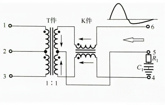
The above figure illustrates the attenuation effect of K components on EMI. The EMI from UTP is applied between Pin 6 and Pin 4, and the solid arrow indicates the direction of EMI current. When EMI current passes through the upper and lower coils of K-piece, its current direction is the same, that is, both currents flow towards the same end. The magnetic flux changes caused by them inside the magnetic ring of K-piece are superimposed on each other, and the inductance presented by K-piece increases linearly with the frequency f.
The inductive reactance is expressed as ZL=2 π * f * L. Among them, L is the inductance of K pieces. At present, the inductance of K components in network transformers produced by various manufacturers is about 10 μ m.
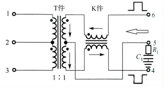
The K-piece is connected in series in the EMI circuit, because a considerable portion of the EMI from UTP needs to drop at both ends of the K-piece before reaching the secondary coil of the T-piece, so the common mode choke can play a role in blocking EMI. The blocking effect of K-piece on the mid to high frequency components of EMI is better, because the higher the frequency f, the larger the ZL, and the greater the EMI at both ends of K-piece.
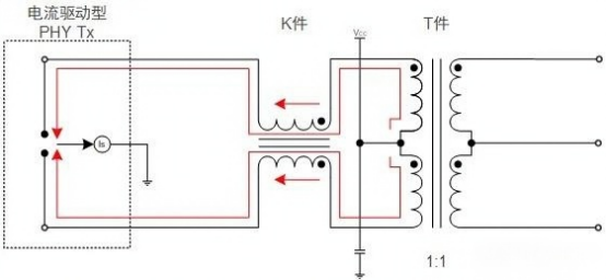
For current type PHY, common mode inductance cannot be placed on the PHY side. The reason is that the current IS flows from the center tap to one or the other winding of the common mode choke coil according to the switch state, and the current is provided by the bias voltage VCC. The PHY chip controls the flow of current. When the instantaneous current of a normal data signal passes through one or two coils, the changes in magnetic flux inside the K-piece magnetic ring are superimposed and not zero, which means that the K-piece will generate high impedance to the normal signal, thereby affecting the transmission of the normal signal.
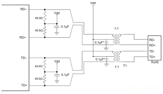
As shown in the figure, it is a typical circuit of current type PHY. There are no K components here, but not all cases require the use of network transformers with K components. The decision to use them is based on EMI test results, cost, and other factors. When laying out this circuit, a 0.1 μ F capacitor should be placed near the center tap of the network transformer, while a 49.9 Ω terminal resistor should be placed near the port of the PHY chip.
- A network transformer consisting of 1.3 T-pieces and K-pieces with three wire loops
The structure of this type of network transformer is not particularly commonly used, but it may be used in certain situations, which will be explained together here. The structural diagram of the network transformer composed of T pieces that can be three wire looped through K pieces is shown in Figure 8. This type of network transformer consists of K pieces, where the two ends of the stimulation coil and the three leads of the middle tap are parallel on the magnetic ring of the K piece, with the same number of turns wound.
As mentioned above, for current type PHY chips, placing K pieces on the PHY side will result in high impedance for normal signals. If K pieces are placed on the UTP side, it will affect the impedance matching of the center tap. Therefore, in order to solve the above problems, a network transformer consisting of T-piece and three wire loop K-piece has emerged. This type of network transformer is suitable for scenarios where K-piece is placed on the PHY chip side. As can be seen from the picture:The instantaneous current of a normal data signal flows out from the terminal, passes through the middle coil, and then enters the PHY chip through the upper and lower coils. In the figure, the total current flowing out through the middle coil is equal in magnitude and opposite in direction, and equal in magnitude and opposite in direction. The total current change in the K pieces of the three wire loop is always zero, that is, the total magnetic flux change is also zero. Therefore, data signals can be transmitted unobstructed in the K pieces of the three wire loop.
The current situation and trends of the network transformer industry.
Detailed explanation of the principle and function of network transformer
Related Article

Practical SMPS transformer calculation tutorial. From parameter confirmation and core selection to winding, air‑gap and thermal verification for power supply design.
How to Calculate Switching Power Supply Transformers: A Complete Method from Parameter Determination to Core Selection

Customized magnetic components are not simple parameter adjustments; they are based on full-dimensional customized design of vehicle application scenarios, operating conditions data, and automotive standards, optimizing from material formulation, magnetic circuit structure, winding process, heat dissipation structure, protection system, and durability verification, completely solving the industry pain points of poor adaptability, short lifespan, and high failure rate of standard components.
How do custom magnetic components ensure longevity in harsh automotive environments?
Unlike ordinary civil‑use power inductors, industrial‑grade inductors for charging piles need to balance anti‑saturation capability, low loss, stability over a wide temperature range, low harmonic interference and excellent heat dissipation performance.
Inductor Selection and Thermal Management Strategy in Charger Module Power Supply: High Efficiency, Stable Load, and Long-Term Reliability Solution
Magnetic components (transformers, common-mode inductors, differential-mode inductors, high-frequency beads) are precisely the core passive devices of BMS for achieving electrical isolation, noise filtering, signal purification, and high-voltage protection.
The isolation and filtering functions of magnetic components in the BMS battery management system
SEND MESSAGE